- 您现在的位置:买卖IC网 > Sheet目录2008 > MAX1135BCAP+ (Maxim Integrated Products)IC ADC 16BIT 150KSPS 20-SSOP
MAX1134/MAX1135
16-Bit ADCs, 150ksps, 3.3V Single Supply
_______________________________________________________________________________________
7
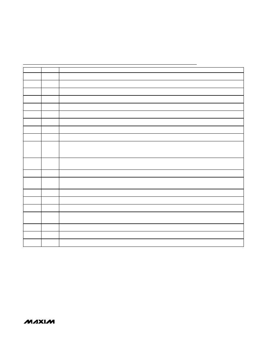
Pin Description
PIN
NAME
FUNCTION
1
REF
ADC Reference Input. Connect a 2.048V voltage source to REF. Bypass REF to AGND with a 4.7F capacitor.
2AVDD
Analog Supply. Connect to pin 4.
3
AGND
Analog Ground. This is the primary analog ground (star ground).
4AVDD
Analog Supply, 3.3V
±5%. Bypass AVDD to AGND (pin 3) with a 0.1F capacitor.
5
DGND
Digital Ground
6
SHDN
Shutdown Control Input. Drive
SHDN low to put the ADC in shutdown mode.
7
P2
User-Programmable Output 2
8
P1
User-Programmable Output 1
9
P0
User-Programmable Output 0
10
SSTRB
Serial Strobe Output. In internal clock mode, SSTRB goes low when the ADC begins a conversion and goes
high when the conversion is finished. In external clock mode, SSTRB pulses high for one clock period before
the MSB decision. It is high impedance when
CS is high in external clock mode.
11
DOUT
Serial Data Output. MSB first, straight binary format for unipolar input, two’s complement for bipolar input.
Each bit is clocked out of DOUT at the falling edge of SCLK.
12
RST
Reset Input. Drive
RST low to put the device in the power-on default mode. See the Power-On Reset section.
13
SCLK
Serial Data Clock Input. Serial data on DIN is loaded on the rising edge of SCLK, and serial data is updated
on DOUT on the falling edge of SCLK. In external clock mode, SCLK sets the conversion speed.
14
DGND
Digital Ground. Connect to pin 5.
15
DVDD
Digital Supply, 3.3V
±5%. Bypass DVDD to DGND (pin 14) with a 0.1F capacitor.
16
DIN
Serial Data Input. Serial data on DIN is latched on the rising edge of SCLK.
17
CS
Chip-Select Input. Drive
CS low to enable the serial interface. When CS is high, DOUT is high impedance. In
external clock mode, SSTRB is high impedance when
CS is high.
18
CREF
Reference Buffer Bypass. Bypass CREF to AGND (pin 3) with a 1F capacitor.
19
AGND
Analog Ground. Connect to pin 3.
20
AIN
Analog Input
发布紧急采购,3分钟左右您将得到回复。
相关PDF资料
MAX1138LEEE+T
IC ADC 10BIT SERIAL 16-QSOP
MAX1159AEUI+
IC ADC 14BIT 135KSPS 28-TSSOP
MAX11602EEE+
IC ADC SERIAL 8BIT 8CH 16-QSOP
MAX11610EEE+T
IC ADC SERIAL 10BIT 12CH 16-QSOP
MAX11616EEE+T
IC ADC SERIAL 12BIT 12CH 16-QSOP
MAX1162AEUB+T
IC ADC 16BIT 200KSPS 10-MSOP
MAX11637EEE+T
IC ADC 12BIT 8CH 16QSOP
MAX11643EEG+T
IC ADC 8BIT 8CH 24QSOP
相关代理商/技术参数
MAX1135BCAP+T
功能描述:模数转换器 - ADC 16-Bit 150ksps 3.3V Single Supply RoHS:否 制造商:Texas Instruments 通道数量:2 结构:Sigma-Delta 转换速率:125 SPs to 8 KSPs 分辨率:24 bit 输入类型:Differential 信噪比:107 dB 接口类型:SPI 工作电源电压:1.7 V to 3.6 V, 2.7 V to 5.25 V 最大工作温度:+ 85 C 安装风格:SMD/SMT 封装 / 箱体:VQFN-32
MAX1135BCAP-T
功能描述:模数转换器 - ADC RoHS:否 制造商:Texas Instruments 通道数量:2 结构:Sigma-Delta 转换速率:125 SPs to 8 KSPs 分辨率:24 bit 输入类型:Differential 信噪比:107 dB 接口类型:SPI 工作电源电压:1.7 V to 3.6 V, 2.7 V to 5.25 V 最大工作温度:+ 85 C 安装风格:SMD/SMT 封装 / 箱体:VQFN-32
MAX1135BEAP
功能描述:模数转换器 - ADC RoHS:否 制造商:Texas Instruments 通道数量:2 结构:Sigma-Delta 转换速率:125 SPs to 8 KSPs 分辨率:24 bit 输入类型:Differential 信噪比:107 dB 接口类型:SPI 工作电源电压:1.7 V to 3.6 V, 2.7 V to 5.25 V 最大工作温度:+ 85 C 安装风格:SMD/SMT 封装 / 箱体:VQFN-32
MAX1135BEAP+
功能描述:模数转换器 - ADC 16-Bit 150ksps 3.3V Single Supply RoHS:否 制造商:Texas Instruments 通道数量:2 结构:Sigma-Delta 转换速率:125 SPs to 8 KSPs 分辨率:24 bit 输入类型:Differential 信噪比:107 dB 接口类型:SPI 工作电源电压:1.7 V to 3.6 V, 2.7 V to 5.25 V 最大工作温度:+ 85 C 安装风格:SMD/SMT 封装 / 箱体:VQFN-32
MAX1135BEAP+T
功能描述:模数转换器 - ADC 16-Bit 150ksps 3.3V Single Supply RoHS:否 制造商:Texas Instruments 通道数量:2 结构:Sigma-Delta 转换速率:125 SPs to 8 KSPs 分辨率:24 bit 输入类型:Differential 信噪比:107 dB 接口类型:SPI 工作电源电压:1.7 V to 3.6 V, 2.7 V to 5.25 V 最大工作温度:+ 85 C 安装风格:SMD/SMT 封装 / 箱体:VQFN-32
MAX1135BEAP-T
功能描述:模数转换器 - ADC RoHS:否 制造商:Texas Instruments 通道数量:2 结构:Sigma-Delta 转换速率:125 SPs to 8 KSPs 分辨率:24 bit 输入类型:Differential 信噪比:107 dB 接口类型:SPI 工作电源电压:1.7 V to 3.6 V, 2.7 V to 5.25 V 最大工作温度:+ 85 C 安装风格:SMD/SMT 封装 / 箱体:VQFN-32
MAX1136
制造商:MAXIM 制造商全称:Maxim Integrated Products 功能描述:2.7V to 3.6V and 4.5V to 5.5V, Low-Power, 4-/12-Channel, 2-Wire Serial 10-Bit ADCs
MAX1136_09
制造商:MAXIM 制造商全称:Maxim Integrated Products 功能描述:2.7V to 3.6V and 4.5V to 5.5V, Low-Power, 4-/12-Channel, 2-Wire Serial 10-Bit ADCs